How to Use Laser Cutters for PCB Prototyping

Can PCB be laser cutting machine technology transform your approach to custom PCB prototyping? Absolutely. These machines offer unmatched precision and speed, making them ideal for creating intricate printed circuit board designs. By utilizing laser cutting technology, you can achieve rapid prototyping, significantly reducing production time compared to traditional methods. This efficiency makes it a popular choice for both hobbyists and professionals. Whether you're crafting custom PCBs for a personal project or a commercial application, laser cutters provide a cost-effective solution that enhances your creative possibilities.
Preparing the Board and Files
When you embark on the journey of custom PCB prototyping using laser cutters, preparation is key. This section will guide you through selecting the right materials, designing your PCB layout, and ensuring safety throughout the process.
Selecting the Right Materials
Choosing the appropriate materials for your PCB is crucial for successful laser cutting.
Types of materials suitable for laser cutting
Laser cutters can handle a variety of PCB materials. Common choices include glass-reinforced epoxy laminate sheets (FR-4), PTFE (Teflon), and metal substrates. These materials are ideal due to their durability and compatibility with laser cutting technology. PCB Laser Cutting Machines excel in cutting and engraving these materials with high precision, making them perfect for intricate designs.
Considerations for material thickness and properties
Material thickness and properties significantly impact the cutting process. Thicker materials may require adjustments in laser settings to ensure clean cuts. Consider the thermal properties of your chosen material, as some may warp under intense heat. A Precision Laser Cutter can efficiently manage different thicknesses, providing accurate results without compromising the material's integrity.
Designing the PCB Layout
A well-designed PCB layout is essential for effective laser cutting.
Software tools for PCB design
Several software tools can assist you in creating your PCB layout. Popular options include Eagle, KiCad, and Altium Designer. These tools offer features that simplify the design process, allowing you to create complex circuits with ease. They also provide options to simulate your design, ensuring functionality before proceeding to the cutting stage.
Exporting design files for laser cutting
Once your design is complete, export it in a format compatible with your laser cutter. Common file formats include DXF, SVG, and Gerber files. Ensure that your design files are precise and error-free to avoid issues during the cutting process. Proper file preparation is crucial for achieving the desired results in your custom PCB prototyping.
Safety Precautions
Safety should always be a priority when working with laser cutters.
Personal protective equipment
Wearing appropriate personal protective equipment (PPE) is essential. Safety goggles protect your eyes from laser exposure, while gloves safeguard your hands from sharp edges and hot materials. Ensure you have adequate ventilation in your workspace to prevent inhalation of fumes generated during the cutting process.
Safe handling of materials and equipment
Handle all materials and equipment with care. Secure the PCB material firmly in the laser cutter to prevent movement during cutting. Regularly inspect your laser cutter for any signs of wear or damage. Following these precautions ensures a safe and efficient cutting process, allowing you to focus on creating high-quality PCBs.
Setting Up the Laser Cutter
Setting up your laser cutter correctly is crucial for achieving high precision in PCB prototyping. This section will guide you through configuring the machine and loading the material effectively.
Configuring the Machine
Proper configuration of the laser cutter ensures optimal performance and precision.
Adjusting laser settings for different materials
You must adjust the laser settings based on the material you are using. Different materials require specific power and speed settings to achieve clean cuts. For instance, FR-4 and PTFE may need different laser intensities. Refer to the manufacturer's guidelines for recommended settings. This step is vital to prevent damage to the material and ensure a smooth cutting process.
Calibrating the laser cutter for precision
Calibration is essential for maintaining the accuracy of your cuts. Begin by checking the alignment of the laser beam. Use calibration tools provided with your machine to fine-tune the laser's focus. Regular calibration helps in achieving consistent results, especially when working on intricate PCB designs. This process ensures that your laser cutter operates at its best, providing the precision needed for detailed work.
Loading the Material
Loading the material correctly is as important as configuring the machine.
Securing the board in the laser cutter
Secure the PCB material firmly in the laser cutter. Use clamps or adhesive mats to hold the board in place. This prevents any movement during the cutting process, which could lead to errors. A stable setup is crucial for achieving precise cuts and engravings.
Ensuring proper alignment and focus
Align the material accurately within the laser cutter. Use the machine's alignment tools to position the board correctly. Ensure the laser is focused on the surface of the material. Proper alignment and focus are key to achieving high precision in your PCB designs. This step minimizes the risk of misalignment and ensures that the laser cutter performs efficiently.
Expert Testimony:
"PCB laser cutting is fast, precise, and the most effective circuit board manufacturing method. Compared to mechanical cutting, PCB laser cutting is the most productive."
By following these steps, you can set up your laser cutter to produce high-quality PCBs with ease. The ability to use a can PCB be laser cutting machine effectively opens up new possibilities for both hobbyists and professionals, offering a cost-effective and efficient solution for PCB prototyping.
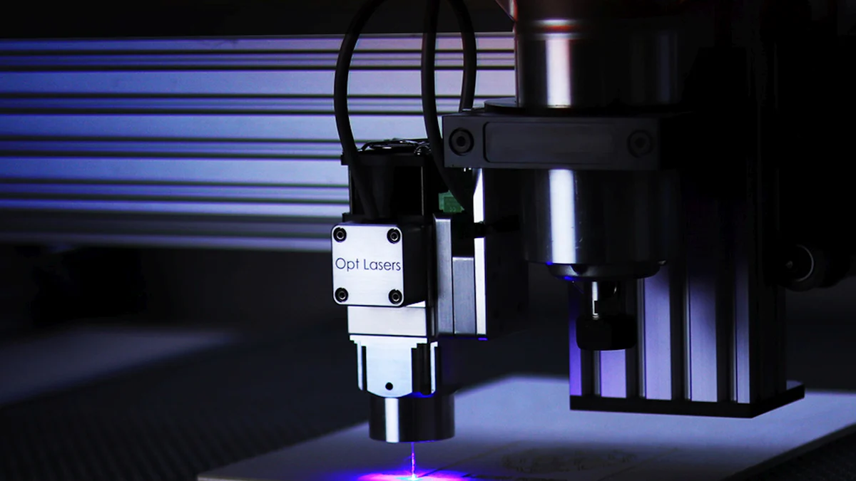
Executing the Cutting and Engraving Process
In this section, you will learn how to execute the cutting and engraving process using a laser cutter. This step is crucial for achieving the desired precision and detail in your PCB designs.
Initiating the Cutting Process
To begin the cutting process, you need to start the laser cutter with the prepared files. Ensure that your design files are loaded correctly into the machine. This step involves selecting the appropriate file format, such as DXF or Gerber, which you have already prepared during the design phase. Once the files are ready, initiate the cutting process by following the machine's operational instructions.
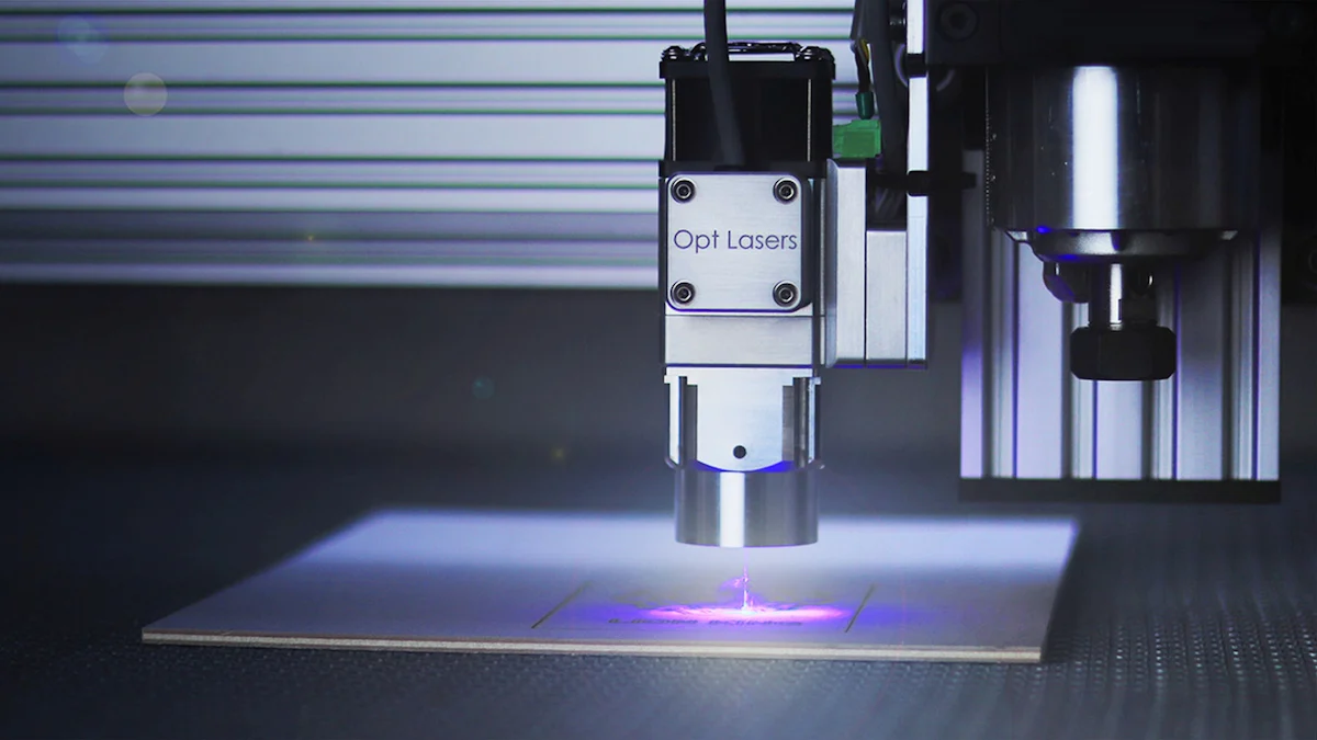
Monitoring the cutting process for accuracy is essential. Keep a close eye on the laser cutter as it works through your design. Watch for any signs of misalignment or errors in the cutting path. If you notice any issues, pause the machine and make necessary adjustments. This vigilance ensures that your PCB maintains high precision throughout the cutting process.
Engraving Details
Engraving fine details on your PCB requires specific techniques. You can achieve intricate designs by adjusting the laser settings to suit the material and design complexity. For example, reducing the laser power and speed can help in etching delicate patterns without damaging the board. Experiment with different settings to find the optimal balance for your project.
Adjusting settings for different engraving depths is another important aspect. Depending on your design requirements, you may need to vary the depth of the engravings. Use the laser cutter's control panel to modify the depth settings. This flexibility allows you to create multi-layered designs, enhancing the functionality and aesthetics of your PCB.
Historical Insight:
The history of direct laser imaging in printed circuit boards (PCBs) dates back to the early 1990s. This technology has evolved significantly, enabling the creation of precise and intricate prototypes across various industries.
The applications of PCB engraving extend beyond simple circuit designs. Industries such as telecommunications and automotive rely on this technology for rapid prototyping of advanced electronic components. The shift towards electric and autonomous vehicles has further increased the demand for high-precision PCB manufacturing.
By mastering the cutting and engraving process, you can leverage the capabilities of a can PCB be laser cutting machine to produce high-quality prototypes. This technology not only enhances your creative possibilities but also plays a vital role in the fabrication of electronic components.
Cleaning and Finishing the Board
After you complete the cutting and etching process, cleaning and finishing your PCB is essential. This step ensures that your board is ready for assembly and functions as intended.
Removing Residue and Debris
Laser cutting and etching can leave behind residue and debris on your PCB. You need to clean these remnants to ensure a smooth surface.
Tools and methods for cleaning the board
To clean your PCB, gather the right tools. Use a soft brush or compressed air to remove loose debris. For stubborn residue, apply isopropyl alcohol with a lint-free cloth. This method effectively cleans the board without damaging it. Ensure you handle the board gently to avoid scratching the surface.
Ensuring a smooth surface for assembly
A smooth surface is crucial for successful assembly. Inspect the board for any remaining particles or rough edges. Use fine-grit sandpaper to smooth out any imperfections. This step prepares the board for component placement and soldering, ensuring a reliable connection.
Inspecting the Cut and Engraving
Inspection is a vital part of the finishing process. You must check the precision and completeness of your cuts and engravings.
Checking for precision and completeness
Examine your PCB closely. Look for clean cuts and accurate engravings. Verify that all design elements are present and correctly executed. Use a magnifying glass to inspect intricate details. This careful examination ensures that your board meets the design specifications.
Making necessary adjustments or corrections
If you find any issues, make the necessary adjustments. Use a laser cutter to correct minor errors. For more significant problems, you may need to cut boards and etch again. Addressing these issues now prevents complications during assembly and testing.
By following these steps, you ensure that your PCB is clean, precise, and ready for the next stage. A well-finished board enhances the overall quality and functionality of your project. The ability to use a can PCB be laser cutting machine effectively allows you to achieve professional results in your prototyping endeavors.
Assembling the PCB
Assembling your PCB is a crucial step in bringing your prototype to life. This process involves soldering components onto the board and testing the prototype to ensure it functions as intended. By following these steps, you can create a reliable and efficient PCB for your project.
Soldering Components
Soldering is the process of attaching electronic components to your PCB. It requires precision and care to ensure a strong connection.
Preparing components for assembly
Before you begin soldering, gather all the necessary components. Organize them according to your PCB layout. This preparation helps you work efficiently and reduces the risk of errors. Inspect each component for any damage or defects. Ensure that the leads are clean and free from oxidation. Proper preparation sets the foundation for successful soldering.
Techniques for effective soldering
Effective soldering requires the right technique. Start by heating the soldering iron to the appropriate temperature. Touch the iron to the pad and component lead simultaneously. Apply solder to the joint, allowing it to flow evenly. Remove the iron once the solder has melted and formed a solid connection. Avoid using too much solder, as it can create bridges between pads. Practice makes perfect, so take your time to master this skill.
Expert Insight:
"Laser cutting enables the creation of precise and intricate prototypes for various industries such as telecommunications, computer and electronic industry, OEMs, industrial, aerospace, automotive, and more."
Testing the Prototype
Testing your PCB prototype is essential to verify its functionality. This step ensures that your design works as intended and identifies any issues that need correction.
Methods for testing functionality
To test your PCB, use a multimeter to check for continuity and correct voltage levels. Power the board and observe its behavior. Ensure that all components function as expected. For complex designs, consider using an oscilloscope to analyze signal integrity. Testing helps you confirm that your PCB meets the design specifications.
Troubleshooting common issues
If you encounter issues during testing, troubleshoot systematically. Check for solder bridges or cold joints that may cause shorts or open circuits. Verify component placement and orientation. Use the schematic to trace connections and identify any discrepancies. Addressing these issues promptly ensures that your PCB operates reliably.
Historical Insight:
The rapid prototyping of PCBs using fiber laser engravers allows designers to quickly iterate and test their designs, enhancing the efficiency of the development process.
By assembling and testing your PCB with care, you ensure that your prototype is ready for real-world applications. This meticulous approach to prototyping not only enhances the quality of your project but also prepares you for future iterations and improvements.
Advantages and Applications of Laser Cutters in PCB Prototyping
Laser cutters have transformed the way you approach PCB prototyping, offering numerous advantages over traditional methods. This section explores the benefits and real-world applications of using laser cutters in PCB design.
Benefits Over Traditional Methods
Speed and efficiency
When you use a laser cutter for PCB creation, you experience unmatched speed and efficiency. Traditional methods often involve multiple steps and manual interventions, which can slow down the process. In contrast, laser cutting streamlines the workflow, allowing you to produce intricate designs quickly. The precision of laser technology ensures that each cut is accurate, reducing the need for rework and saving valuable time.
Cost savings and material conservation
Laser cutting not only speeds up the process but also offers significant cost savings. By minimizing material waste, you conserve resources and reduce expenses. Traditional methods often result in excess material loss due to imprecise cuts. Laser cutters, however, use advanced technology to optimize material usage, ensuring that you get the most out of your PCB materials. Over time, these savings add up, making laser cutting a cost-effective choice for both hobbyists and professionals.
Real-World Applications
Use cases in various industries
Laser cutters find applications across a wide range of industries. In telecommunications, they enable the rapid prototyping of complex circuit boards, essential for developing new communication devices. The automotive industry relies on laser cutting for creating precise PCBs used in modern vehicles, including electric and autonomous models. Aerospace companies benefit from the technology's ability to produce lightweight and reliable electronic components. These examples highlight the versatility of laser cutters in meeting diverse industry needs.
Examples of successful projects
Numerous successful projects demonstrate the effectiveness of laser cutters in PCB prototyping. For instance, a startup developing wearable technology used laser cutting to create compact and efficient circuit boards, accelerating their product development timeline. In another case, an educational institution incorporated laser cutting into their engineering curriculum, allowing students to design and fabricate their own PCBs. These projects showcase how laser cutters empower innovation and creativity, enabling you to bring your ideas to life with precision and speed.
By understanding the advantages and applications of laser cutters in PCB prototyping, you can leverage this technology to enhance your projects. Whether you're working on a personal hobby or a professional endeavor, laser cutters provide the tools you need to achieve high-quality results efficiently.
Using laser cutters for PCB prototyping offers a streamlined process that enhances precision and efficiency. You can follow key steps such as preparing the board, setting up the laser cutter, and executing the cutting process to achieve high-quality results. This technology revolutionizes prototyping by allowing rapid iteration and testing of intricate designs. Explore laser cutting for your PCB projects to unlock new creative possibilities. The potential for innovation in PCB design is vast, making laser cutting an invaluable tool for both hobbyists and professionals.
FAQ
What is a PCB?
A PCB, or Printed Circuit Board, is a board used to mechanically support and electrically connect electronic components. It consists of conductive pathways etched from copper sheets laminated onto a non-conductive substrate. PCBs are essential in modern electronics, providing a compact and efficient way to organize and connect components.
Can I use any laser cutter for PCB prototyping?
Not all laser cutters are suitable for PCB prototyping. You need a laser cutter that can handle the specific materials used in PCBs, such as FR-4 or PTFE. Fiber lasers are effective for engraving copper layers, while CO2 lasers are better for cutting the board material. Always check the specifications of your laser cutter to ensure compatibility with PCB materials.
How do I choose the right material for my PCB?
Selecting the right material depends on your project's requirements. Common materials include FR-4, known for its durability and thermal resistance, and PTFE, valued for its high-frequency performance. Consider factors like thickness, thermal properties, and the specific application of your PCB when choosing a material.
What software should I use for designing PCBs?
Several software tools are available for PCB design, each offering unique features. Popular options include Eagle, KiCad, and Altium Designer. These tools help you create detailed layouts and simulate your designs before cutting. Choose software that fits your skill level and project needs.
How do I ensure safety when using a laser cutter?
Safety is crucial when operating a laser cutter. Always wear safety goggles to protect your eyes from laser exposure. Use gloves to handle sharp edges and hot materials. Ensure your workspace is well-ventilated to avoid inhaling fumes. Regularly inspect your equipment for wear and damage to maintain a safe working environment.
What are the benefits of using laser cutters for PCB prototyping?
Laser cutters offer several advantages over traditional methods. They provide high precision and speed, allowing you to create intricate designs quickly. Laser cutting reduces material waste, saving costs. This technology also enables rapid prototyping, helping you iterate and test designs efficiently.
Can laser cutters handle complex PCB designs?
Yes, laser cutters excel at handling complex designs. Their precision allows for fine details and intricate patterns that might be challenging with traditional methods. By adjusting laser settings, you can achieve various engraving depths and create multi-layered designs, enhancing both functionality and aesthetics.
How do I clean my PCB after laser cutting?
After cutting, clean your PCB to remove residue and debris. Use a soft brush or compressed air for loose particles. For stubborn residue, apply isopropyl alcohol with a lint-free cloth. Ensure the board is smooth and free of imperfections before assembly.
How do I test my PCB prototype?
Testing ensures your PCB functions as intended. Use a multimeter to check for continuity and correct voltage levels. Power the board and observe its behavior. For complex designs, an oscilloscope can help analyze signal integrity. Address any issues promptly to ensure reliable operation.
What industries benefit from laser-cut PCBs?
Many industries benefit from laser-cut PCBs, including telecommunications, automotive, and aerospace. These sectors rely on precise and efficient PCB manufacturing for developing advanced electronic components. Laser cutting supports innovation and rapid prototyping, meeting diverse industry needs.
See Also
Maximizing Efficiency with Your Laser Cutting Machine
Guide to Metal Cutting Using a Desktop CNC
Rapid Circuit Board Cutting with Advanced Machinery